As the RF industry trends towards ever higher frequencies, integration and complex digital modulations to satisfy demands for exploding wireless data throughput, small size, and low power consumption; RF circuit and system designers now must design compact components for millimeter wave applications with digital modulations such as 5G wireless (24 to 53 GHz), automotive radars (76 – 81 GHz) and WiGig networking (60GHz). Such components are called RF modules which integrate multi-technology parts such as RFICs, MMICs, laminates, wafer level packaging, printed phased-array antennas, PCBs and RF connectors.
The EDA design flow for multi-technology RF modules must be re-examined to avoid 4 critical pitfalls that can hamper an already challenging design task and cause design failures. These are:
- Assembly and 3D routing of multi-technology modules without errors
- Extract and analyze portions of 3D module layout and interconnected active/passive components with EM-circuit cosimulation without invasive cookie cutting
- Tuning and optimizing RF circuits for EVM (error vector magnitude) to directly satisfy digital RF modulation performance without inferring from classic analog P1dB and IP3
- Guarantee and fix amplifier stability under all linear, nonlinear and load conditions with a single schematic analysis instead of using 14 separate schematics and analysis
1. Multi-Technology RF Assembly & Integration
The EDA platform to design multi-technology RF modules must be able to read, assemble, rout, and verify integrated IC and PCB design databases representing the combination of:
- RFIC, chip scale packaging and antenna layouts based on OA (e.g. Virtuoso, EMPro)
- PCB and laminate layouts based on ODB++ (e.g. Allegro, Expedition, Zuken)
- ADS (Advanced Design System) native MMIC and RF layouts
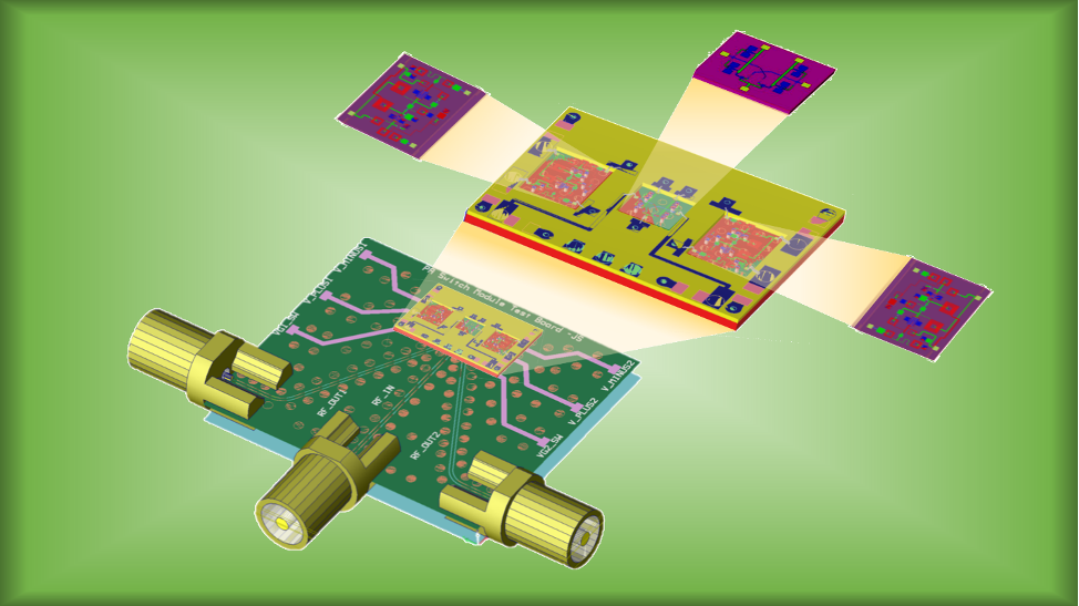
An example of this drag-&-drop assembly technology is called SmartMount from Keysight ADS that automatically handles different units (e.g., um & nm for ICs; mm, mils & inches for PCBs/laminates), orientation (top/bottom mount, flip chip, etc.), and different technology layer stack up definitions of each design.
3D avoidance routing and editing of RF interconnects through the assembled multi-technology structure is then needed for the RF signals to flow. The correctness of assembly and routing is verified by module level DRC (design rule check), LVS (layout-vs-schematic) and LVL (layout-vs-layout) across multi-technology boundaries. This requirement makes traditional IC-only or PCB-only EDA tools obsolete for multi-technology design.
2. Automatic Layout-Circuit Extraction for 3DEM-Circuit Simulation
Correct multi-technology assembly and routing must still have good RF performance. Critical RF signal paths interconnected across technology boundaries must be checked for loss, coupling, mismatches, isolation, and frequency shifts. RF designers need to quickly extract these 3D RF paths or electrical nets for 3D EM-circuit cosimulation to ensure EM (electromagnetic) effects from physical interconnects are accounted for.
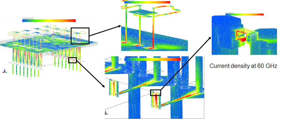
Traditionally this kind of 3D EM-circuit cosimulation is very tedious and error-prone to setup such as invasive cookie cutting the layout, stripping out circuit components, assigning ports and ground references for every circuit node and stitching the EM S-parameter ports result back to the circuit nodes correctly. For circuits with hundred of ports, it is very easy to make a manual re-connection mistake that leads to a costly failed design downstream.
RFPro is an industry-first breakthrough in 3D EM-circuit cosimulation capability that enables RF circuit designers to interactively run EM analysis on any selected RF signal path or nets without cookie cutting and tedious setup. Since no modification of the layout or schematic is needed, 3D EM-circuit simulation can be done effortlessly for design tuning and optimization. It also preserves the integrity of the original design to avoid introducing manual modification errors from using standalone 3DEM simulators.
3. Circuit EVM (Error Vector Magnitude) for Digital Modulated RF
5G, automotive radar, WiFi 6E, IoT…, almost all modern wireless applications employ digitally modulated signals. EVM (Error Vector Magnitude) is now the common figure of merit for measuring the performance of a circuit or system under digital modulation stimulus. With increasing signal bandwidth and modulation density, the traditional rule of thumb such as P1dB or IP3 as an indicator of EVM performance are no longer valid. But EVM analysis at the circuit level was too slow to be useful as a design tool for tuning and optimization because of the need for demodulating the digital RF signal.
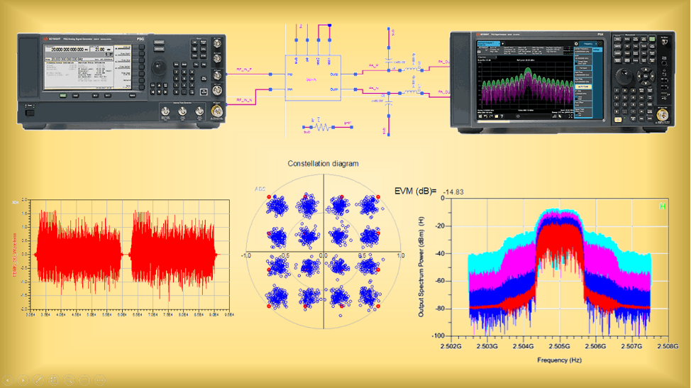
Fortunately, Keysight instrumentation and simulators now employ spectrally equivalent compact test signals to derive EVM measurements at 10-100x faster speed and without the need for demodulation.
To achieve early design wins for a specific application in a competitive market, verification of circuit designs against industry wireless standards such as 5G, WiFi, automotive radars, etc. requires a library of test with standards-compliant modulated sources and companion demodulation algorithms. The algorithms used for signal generation and demodulation should be consistent between instrumentation and simulation to verify that the design works before hardware fabrication to shorten time-to-market. Keysight is the only known EDA vendor that provides these verification test benches (VTBs) to help achieve design wins.
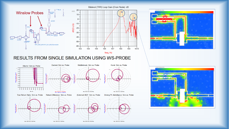
4. Guarantee Nonlinear Amplifier Stability
With 5G and automotive radar frequencies trending towards 40 GHz and 77 GHz respectively, transistor gain must also increase to offset high frequency gain roll off. High transistor gain together with increased parasitic coupling from densely integrated RF modules often results in unstable amplifiers.
Amplifier designers have often wished for a single all-encompassing stability analysis that can determine whether an amplifier is unstable or not under both large and small signal excitations with different load conditions.
The Winslow stability analysis in ADS has finally made that possible by replacing 14 traditional different schematic setup and analysis with just one, but still comprehensively produces all the stability analysis results. When an amplifier is found to be unstable, it is also possible to determine the location and cause of instability so that you can fix it by using a combination of RFPro and Winslow analysis as the figure below shows.
Make sure your EDA tool fulfills these 4 critical requirements to avoid pitfalls in your RF design flow for 5G and other mmWave applications that cause costly rework and lose lucrative design wins to your competition.